
Comprehensive Technical Guide to Rhenium-Tungsten (Re-W) Probes
I. Introduction-Rhenium-Tungsten Probes
While Tungsten is a metal known for its extreme hardness and high-temperature resistance—making it a staple for filaments, electrodes, thermocouples, and probes—it suffers from inherent brittleness and low ductility, which significantly limits its service life. To mitigate these drawbacks, traditional metallurgical methods involve adding rare metals to form tungsten-based alloys.
In the semiconductor testing industry, Re-W probes serve as an upgraded version of pure tungsten probes. The addition of 3% or 5% Rhenium fundamentally transforms the material's physical characteristics:
l Overcoming Brittleness: It resolves the issue of room-temperature brittleness and susceptibility to fracture found in pure tungsten.
l Enhanced Hardness: It improves wear resistance, thereby extending the test life cycle.
l High-Temperature Resistance: It raises the recrystallization temperature, ensuring mechanical stability during continuous high-current or high-temperature testing.
The addition of Rhenium triggers the "Rhenium Ductilizing Effect," which vastly increases the plasticity of Tungsten. Re-W alloys boast a suite of superior properties: high melting point, high strength, high hardness, high ductility, high recrystallization temperature, high resistivity, low vapor pressure, low electron work function, and a low ductile-to-brittle transition temperature.
The apex of a Rhenium-Tungsten probe is manufactured using specialized processes, ensuring high taper precision and a high modulus of elasticity. The resulting product is more resistant to wear and corrosion, featuring a smooth, damage-free surface with a finish (Ra) below 0.25, achieving a near-mirror effect.
II. Models & Specifications
Re-W probe specifications are typically customized based on the requirements of Probe Card designs or Probe Station setups.
1. Common Material Grades
l WRe 3% (3% Re, 97% W): The industry-standard grade. It balances extreme hardness with excellent toughness, suitable for most logic and memory chip testing.
l WRe 5% (5% Re, 95% W): Offers higher tensile strength and superior corrosion resistance, often utilized in specialized high-temperature testing environments.
2. Core Technical Specifications
|
Parameter |
Specification Range (Typical) |
Description |
|
Shank Diameter |
0.05mm - 1.2mm (Common: 5mil, 7mil, 10mil) |
Determines the overall rigidity of the probe. |
|
Tip Radius |
0.08μm (Ultra-sharp) to 100μm (Radius) |
Selected based on the size of the Pad under test. |
|
Overall Length |
15mm - 300mm |
Depends on the probe fixture or probe card thickness. |
|
Taper Angle |
3° - 15° |
Affects the elastic modulus and visual alignment. |
|
Hardness |
600 - 900 HV |
Higher than pure tungsten; offers superior wear resistance. |
|
Surface Finish |
Polished (Ra < 0.25) or Coated |
Reduces aluminum/solder debris accumulation. |
3. Tip Style Classification
l Sharp Tip: Used for micro-pads or applications requiring penetration of oxide layers.
l Flat Tip: Used for large-area contact to reduce current density.
l Radius (Round) Tip: Reduces scratching on the chip surface to protect the Device Under Test (DUT).
III. Key Advantages
l High Wear Resistance: The hardness of Re-W alloy exceeds that of pure tungsten, meaning the tip shape is better maintained after thousands of contact cycles, lowering the total cost of test.
l Enhanced Toughness: The addition of Rhenium lowers the ductile-to-brittle transition temperature, making the probe less likely to snap under lateral force or overdrive.
l Anti-Oxidation & Anti-Carbon Accumulation: When testing aluminum pads, Re-W probes effectively reduce debris accumulation (clogging), maintaining stable contact resistance.
l Superior Electrical Performance: Features low and stable Contact Resistance (Rc), ensuring the integrity of signal transmission.
IV. Uses & Functions
Rhenium-Tungsten probes act as a "bridge" in the electronics production chain:
l Electrical Connection: Establishes a temporary, reliable electrical path between the Tester and the Device Under Test (DUT).
l Signal Extraction: Collects micro-current and voltage signals from the wafer to determine chip functionality.
l Failure Analysis (FA): Used in labs with micro-manipulators to probe internal circuits and locate failure points.
l Aging/Burn-in Test: Maintains stable physical contact during prolonged energized testing.
V. Application Fields
1. Wafer Sorting (CP Test): The primary application. Probes are mounted on cantilever probe cards for wafer-level quality inspection before packaging.
2. LCD/OLED Display Testing: Used to check driver IC connections and pixel illumination; requires ultra-fine diameters for high-density pitch.
3. Failure Analysis & R&D: Used by semiconductor design firms and research institutes with manual probers for internal signal probing.
4. Power & RF Testing: Due to thermal stability, they are ideal for high-current power devices (IGBT, SiC) and high-frequency RF chip measurements.
5. Automotive Electronics & MEMS: Testing for airbags, pressure sensors, and other Micro-Electro-Mechanical Systems requiring high durability.
VI. Maintenance & Care Recommendations
l Cleaning: Regularly use specialized cleaning maps (polishing sheets) or ultrasonic cleaning to remove metallic debris from the tip.
l Pressure Control: Strictly adhere to the designed Overdrive limits of the probe card to prevent premature fatigue or tip damage.
l Storage: Store in dry, vibration-proof probe boxes to prevent tips from colliding and deforming.
Conclusion
With high hardness, fatigue resistance, and excellent electrical stability, Rhenium-Tungsten probes have become an indispensable consumable in the semiconductor testing industry. As chip manufacturing advances toward 3nm and 5nm nodes, the requirements for tip precision and material homogeneity of Re-W probes have reached unprecedented levels.
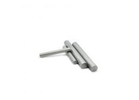
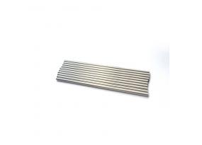
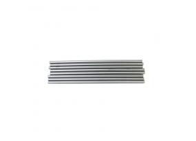
Carbide Rods Products
All Categories
- Ground Solid Tungsten Carbide Rods
- Unground Solid Tungsten Carbide Rods
- Tungsten Carbide Rods Single Hole
- Tungsten Carbide Rods Double Holes
- Nonstandard Tungsten Carbide Rods
- Tungsten Carbide Bars And Strips
- Tungsten Carbide Plates
- Customized Tungsten Carbide Products
- Tungsten Carbide Burr Blank
- Tungsten Weight
- Tungsten carbide rods&Custom-made Carbide rods
- Cemented Carbide Plates & Non-Standard Custom-made Carbide Plates
- Cemented Carbide Strips & Non-Standard Custom-made Carbide Strips
- Cemented Carbide Die & Non-Standard Custom-made Carbide Die
Contact Us
HAO Carbide Co., LTD.
Catherine Tang
Tel: +86-731-22199705
Fax: +86-731-28260602
Mob: +86-13975383023
Email: Catherine@haocarbide.com
Web: www.hao-carbide.com
Address: Building 3, Power Valley Industrial Park, Zhuzhou City, Hunan Province, China